



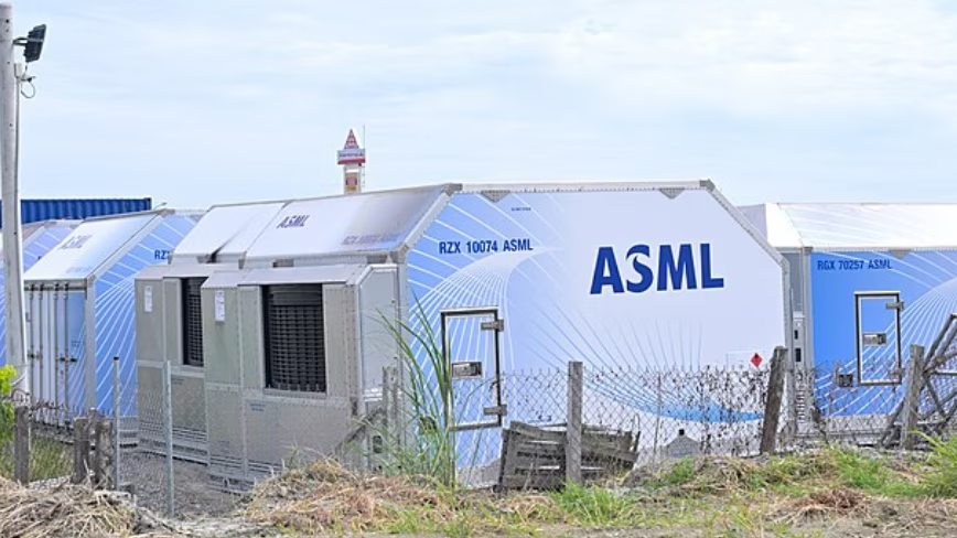

ASML air freight containers in Tainan, May 2025 Credit: 4300streetcar ASML’s most advanced lithography machines cannot print the largest chips the AI industry currently builds. The company now has a plan to change that, and it has brought TSMC in on it. The initiative was reported by Reuters on Tuesday and confirmed the same day in a joint announcement from the two companies. ASML wants to move the industry from the 6-inch photomasks it has used for decades to 12-inch masks, so that its High NA machines can expose a chip the size of today’s biggest data-centre processors in a single shot.
The constraint is optical rather than commercial. High NA systems use anamorphic optics to resolve finer features, and the trade is that they expose roughly half the area of the older generation in one pass. Processors designed by Nvidia and Google already run to about 800 square millimetres, which sits at the ceiling of what the current tools print at once. On a High NA machine, a die that size would have to be stitched together from two exposures, a technique that costs throughput and introduces a seam where yield problems like to live.
A bigger mask removes the need for the seam. The payoff ASML is advertising is throughput. “If we’re going to pull it off as an industry, then you’ll actually see that the productivity of those systems will go up by 40%,” Marco Pieters, the company’s chief technology officer, told Reuters. The phrasing is careful. A mask standard is not something a scanner vendor can change alone.
Which is what makes TSMC’s presence the news. The world’s largest contract chipmaker has been the most conspicuous holdout on High NA, and TNW has covered its scepticism as Intel moved first. The company is now co-signing the roadmap. TSMC chairman and chief executive C.C.
Wei said in a statement that bringing together expertise from across the industry’s value chain was intended to keep delivering cutting-edge technology “through continuous innovation that lowers barriers”. ASML chief executive Christophe Fouquet framed adoption as progressive, starting on 6-inch masks and later supported by 12-inch ones. The dates are worth reading slowly. TSMC intends to use High NA in high-volume manufacturing at advanced nodes from 2030, on the existing 6-inch masks.
A pilot line for 12-inch masks is planned for 2031. The systems are not expected to be ready for advanced-node production until 2033. That is two full process generations away, and the AI chips this is meant to enable do not exist yet either. Others are further along on the machines if not the masks.
Intel is already running High NA in production and has shipped laptop processors made on it, having bought in early when the tools cost roughly $400mn each. Samsung is targeting a High NA introduction for DRAM in 2028, and SK Hynix is weighing whether to join the consortium while aiming at the same year for High NA DRAM in volume. For ASML, the commercial logic is straightforward enough. Every High NA system it sells is worth several times a conventional EUV tool, and the company is already trying to build machines faster because AI demand is running ahead of what its factories can produce.
Committing customers to a mask transition that only pays off on High NA is a way of making the expensive machine the default rather than the exception, well before the decade is out. The reason this needs a consortium rather than a purchase order is that a mask size is infrastructure. Changing it pulls in blank suppliers, pellicle makers, mask writers, inspection and repair tools, and every handling system in a fab, none of which ASML owns. That is a decade of coordinated capital spending across companies that compete with each other, agreed now on the expectation that chips will keep getting bigger.
It is a reasonable bet. It is still a bet.